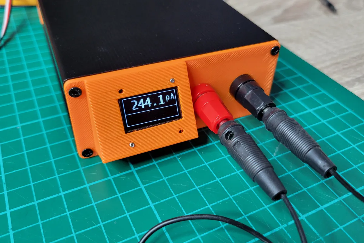

Introduction
This project aims to create a custom power profiler from sub-nA measurement up to 500 mA. It is based on the analog circuitry designed by Dave from EEVBlog in his uCurrentMeter [Link].
Dave’s project requires a multimeter to measure the voltage drop in a shunt resistor, which depends on the range that the device is measuring. The device only works on one range at a time, requiring the user to switch between channels (nanoamperes, microamperes and milliamperes) by a physical switch. Therefore, the uCurrent is ideal only if the current being measured does not require dynamic range switching
For my projects, I need to log the current consumption of devices as they transition between normal operation and low-power modes. Usually my projects are based around STM32 or ESP32 microcontrollers, which requires from hundreds of milliamps in normal mode (e.g.:300mA the ESP32 when using WiFi) down to dozens of microamps for the STM32 low power mode.
The microPowerMeter (Name TBD)
The microPowerMeter is a project aim to add the required extra features to the the circuit in the uCurrent, that is:
- Read current from nA range to mA.
- Automatic channel switch.
- Logging capabilities through USB for later data analysis.
- (Optional) Screen for standalone use.
There are similar other projects:
- Power Profiler Kit (100€): 0.2µA resolution, 200nA to 1A, 100Ksps, 0.8-5 Vcc, includes Logic analyzer.
- Otii Arc Pro (1000€): Accuracy 50nA, 50nA to 2.5A, 4ksps in low current range.
- JouleScope (1000€): 0.5nA resolution, 15V, 3A, 2Msps
There are alternatives to my microPowerMeter, however they lack the range (Power Profiler) or I lack the money (Otii Arc Pro or JouleScope). So, my plan is to create a custom version at lower cost but with the required current range.
Version 1.0 (January 2026)
Design
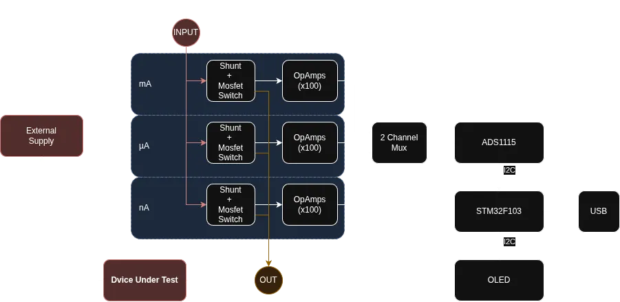
In the first version of the uPM I just wanted to add a microprocessor to get the data and send it to the PC using a USB. The aim in this step is to do an affordable, and easily available components.
From my backgroun in the Maker world, I am used to work with the STM32F103 from which I have some bluepills (Aliexpress) and some ADS1115 (Aliexpress) modules laying around. Also for this version, I also added a typical 0.96 inches OLED screen (Aliexpress) to show the measurements.
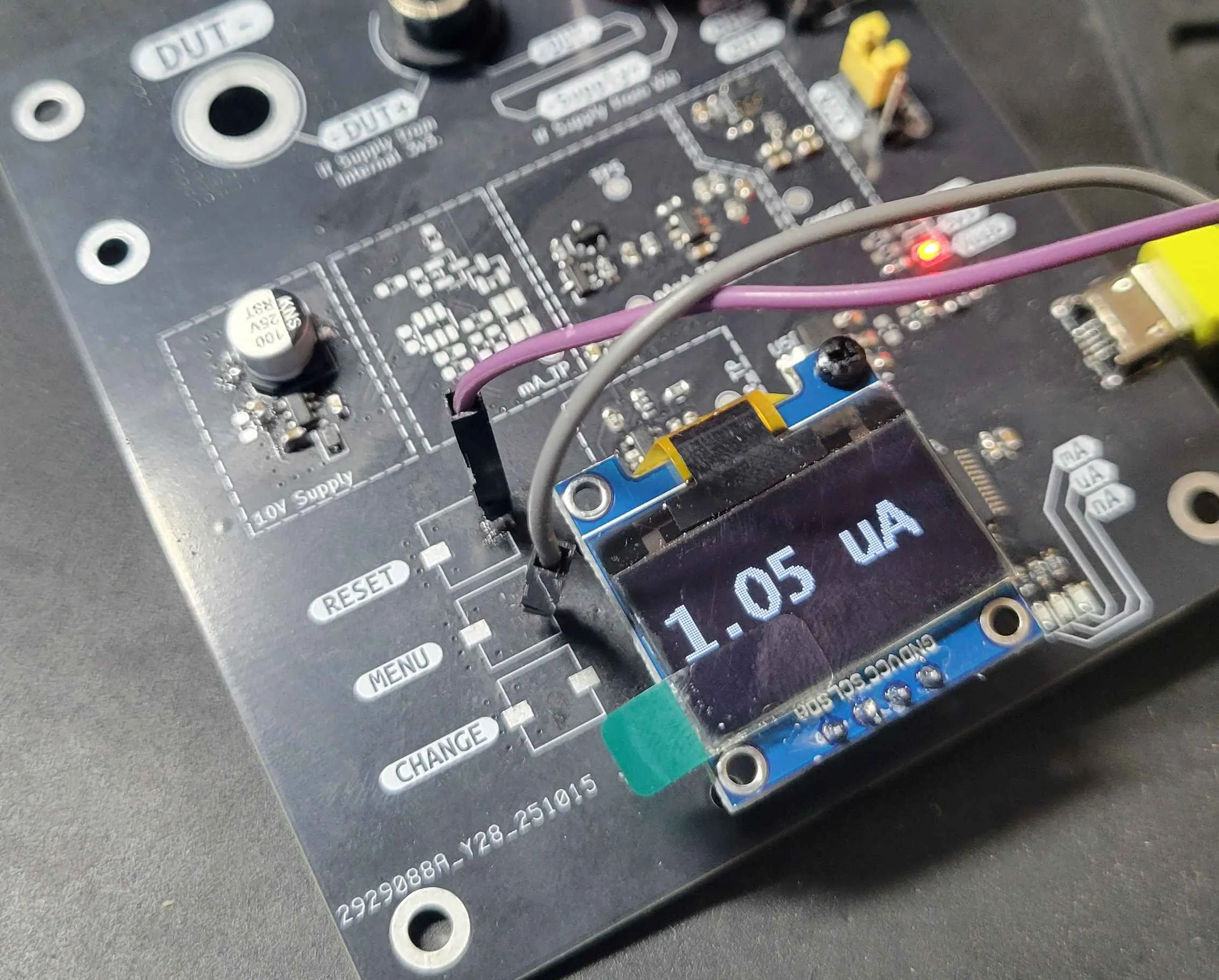
First test and problems.
The STM32F103 main tasks was to read the ADC from the ADS1115, and send it to the Host PC using USB, if you want to know how add Tiny USB support to STM32 microcontrollers you can check this blog post.
Pretty simple design, which actually seems to work in the µA range. However, during extensive testing, the device several issues began to emerge. In the image below, the device is working with 1 µA, but analyzing the data from the PC shows the real thruth. The signal captured by the device contains a high 50Hz signal coupled into the actual signal.
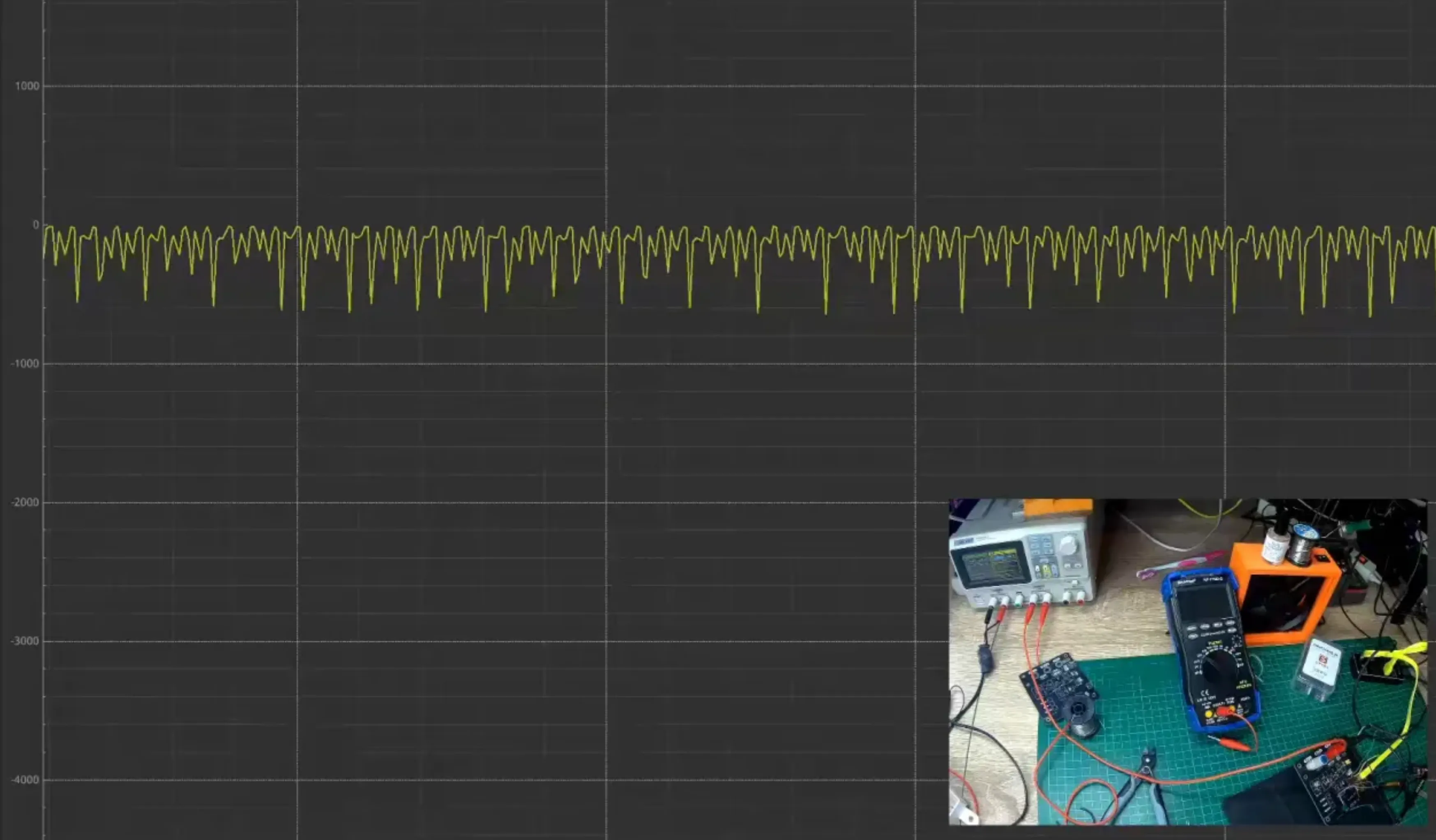
Mains voltage coupling
I had heard about this issue, but never experience myself. When working in regular projects, AC coupling usually is not a problem. The hundreds of microamperes flowing though the circuit do not affect the measurements or the device’s functionalities. However, in this project, the voltage drop in the shunt resistor is in the range of µA in a 10 , even the lowest current can create a measurable noise.
The mains coupling is a problem that appears when the mains frequency (in Spain 50 Hz) is capacitive coupled to the circuit. The circuit, the probes, the cabling, everything couples with the main voltage, thus generating a small AC current flow through the circuit. This small current generates the noise in the measuring shunt.
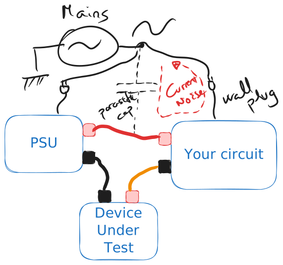
Solving the AC coupling in this first version of the PCB is not easy. The signal bypassing the parasitic capacity to the mains voltage has to come back to the wall plug, and the easiest way is through our measuring circuit.
Version 2.0
Design
In order to solve the AC coupling problem two power domains are created, which are isolated one from another. The two domains are:
- The main domain, which is connected to the Host PC/USB power supply, is the one handling the high speed USB communication and the OLED Display.
- The analog domain, that is connected to the DUT: contains the analog and ADC circuitry to capture the signal.
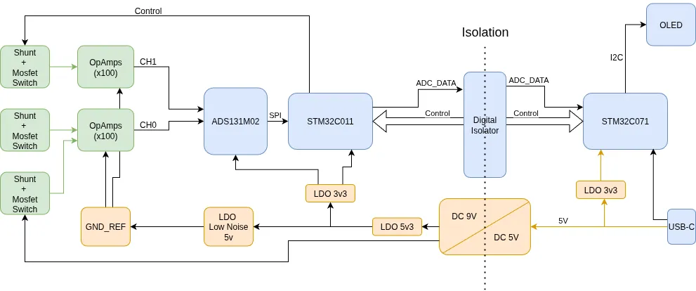
The idea is to gather the ADC samples using the microcontroller in the analog domain, and send them to the main domain so the OLED can show the last value and the Host can log the ADC values. The main domain also can control the analog domain by the use of Control Commands or by resetting the the analog part microcontroller.
Main domain (Non-Isolated)
The main domain, the non-isolated domain, contains the USB and screen, and connects to the Host PC. This domain handles the communication of the ADC data to the Host Computer.
USB Supply
The entry point of the main domain is the USB that provides the power to the device by the VBUS. The USB 5V is then
filtered by a -filter with 100 + 1 µF, and 300 500mA ferrite. The 5V is down converted to 3v3 volts using a
TLV773, a small LDO with High-PSRR.
The main domain does not require a very clean power supply signal, and the requierements are pretty relax. The -filter and the LDO are chosen to be some cheap component.
Another headache was looking for a proper USB-C connector. USB-C is complex and requires a lot of available pins. However, when you look for USB-C sockets, there are sockets for USB 2.0, there are power only connector, one side connectors, and a bunch of other variants.
Warning
When looking for a USB-C carrefully check the connections! Not all USB-C have the same pinout. Also Check the pin ordering in the PCB schematic
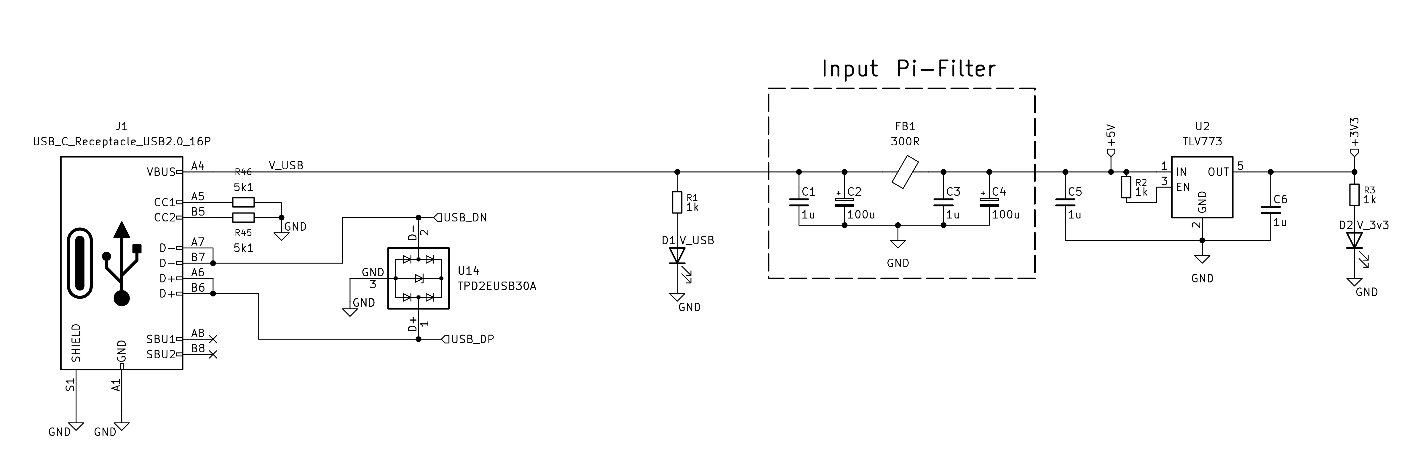
Here you can find a list of the most important parts of this circuit section.
| P.N. | Function | Price |
|---|---|---|
| TLV77333PDBVR | Voltage regulator (LDO) - 5v to 3.3V | 0.10 € |
| MMZ1608S301ATA00 | Ferrite bead 0.3, 500mA | 0.08 € |
| USB-TYPE-C-018 (DEALON) | USB-C Connector | 0.50 € |
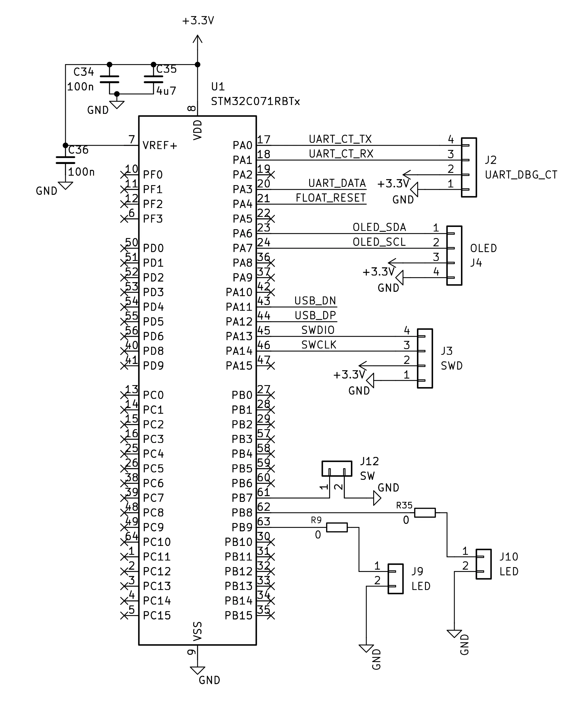
Microcontroller STM32C071
This simple section is just to show the connections available in the STM32C071. The communication with the analog domain
contains two channels: the data channel UART_DATA from which it receives the ADC data, and the control channel UART_CT_RX/TXto being able
to send commands to the analog domain microcontroller. The FLOAT_RESET signal controls the analog domain’s microcontroller
reset pin.
The remaining connectors are:
- OLED: Simple I2C screen.
- SWD : Connector for the ST-Link.
- LEDs: User feedback LEDs.
- SW : Switch for user input if required.
The STM32C071 was chosen due to its low part requirement. It has internal HSI with
clock recovery for crystal-less USB, and only two power pins VDD and VSS. The STM32C071
is a Cortex-M0+ MCU at 48 MHz and has the required peripherals (2x UARTs, 1x I2C) with a
price of 1,27€ per unit ordering 10.
Isolation
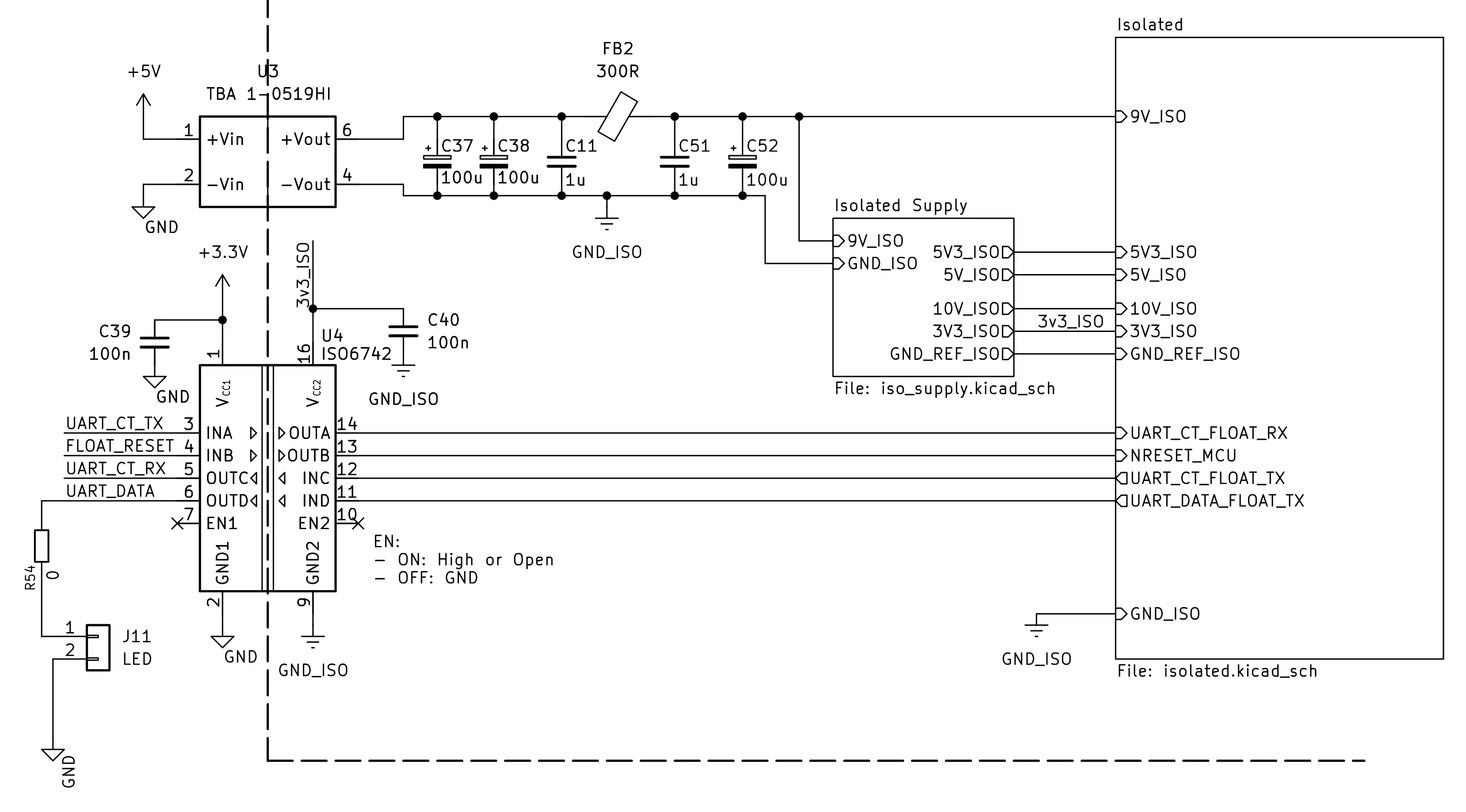
In order to avoid the mains coupling to the circuit, the objective is to send the data and power through an isolation barrier.
The DC/DC converter “moves” the power from one domain to the other. It transforms the DC voltage in input to AC so it can be transfered using a small transformer to the output, and at the output do a simple regulation. However, the output ripple is pretty high, requiring extra filtering at the output.
For the digital signals I am using a ISO6742 isolator which isolates digital signals up to 50 Mbps. We are using 2 lines for UART Control TX and RX; 1 line for ADC Data and the last one for resetting the analog domain.
Analog Domain (Isolated)
Low noise - Isolated Supply
For the analog domain one key aspect of the design is the noise floor. The input comes from the TBA 1-0519HI which has an unregulated
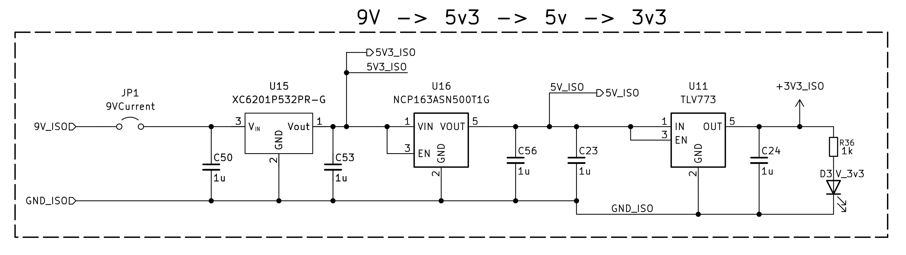
output that has to be regulated. In addition to the capacitors we added at the output of the DC/DC, I have implemented the next chain:
- XC6201P532: High input voltage range. Used to convert the 9V to 5.3V.
- NCP163ASN500T1G: Low noise, high PSRR, used to supply the power to the opAmps.
- TLV773: Regular LDO, used to digital ICs.
This chain may seem overkill, however, during testing we had some problems with the noise floor, that were fixed in this version. The
first regulator job is to lower the voltage and start rejecting the ripple from the DC/DC. The second regulator, the NCP163ASN500T1G, is
a specialized regulator for low noise circuitry, which is ideal for our OpAmp. Since the NCP163ASN500T1G has a very low input voltage limit, we need
the previous XC6201P532.
Lastly the TLV773 is the last regulator for the digital components. Since these components are less susceptible to noise, we can use a
general use linear regulator.
| P.N. | Function | Price |
|---|---|---|
| XC6201P532 | High voltage regulator | 0.53 € |
| NCP163ASN500T1G | Low noise, high PSRR regulator | 0.33 € |
| TLV77333PDBVR | Voltage regulator (LDO) - 5v to 3.3V | 0.10 € |
Amplification Stage
The Amplification part is based on EEVBlog circuit you can check its documentation on the µCurrentGold.
In my version I just added the channel selection using couple of MOSFETS, and some filtering between stages.
ADC
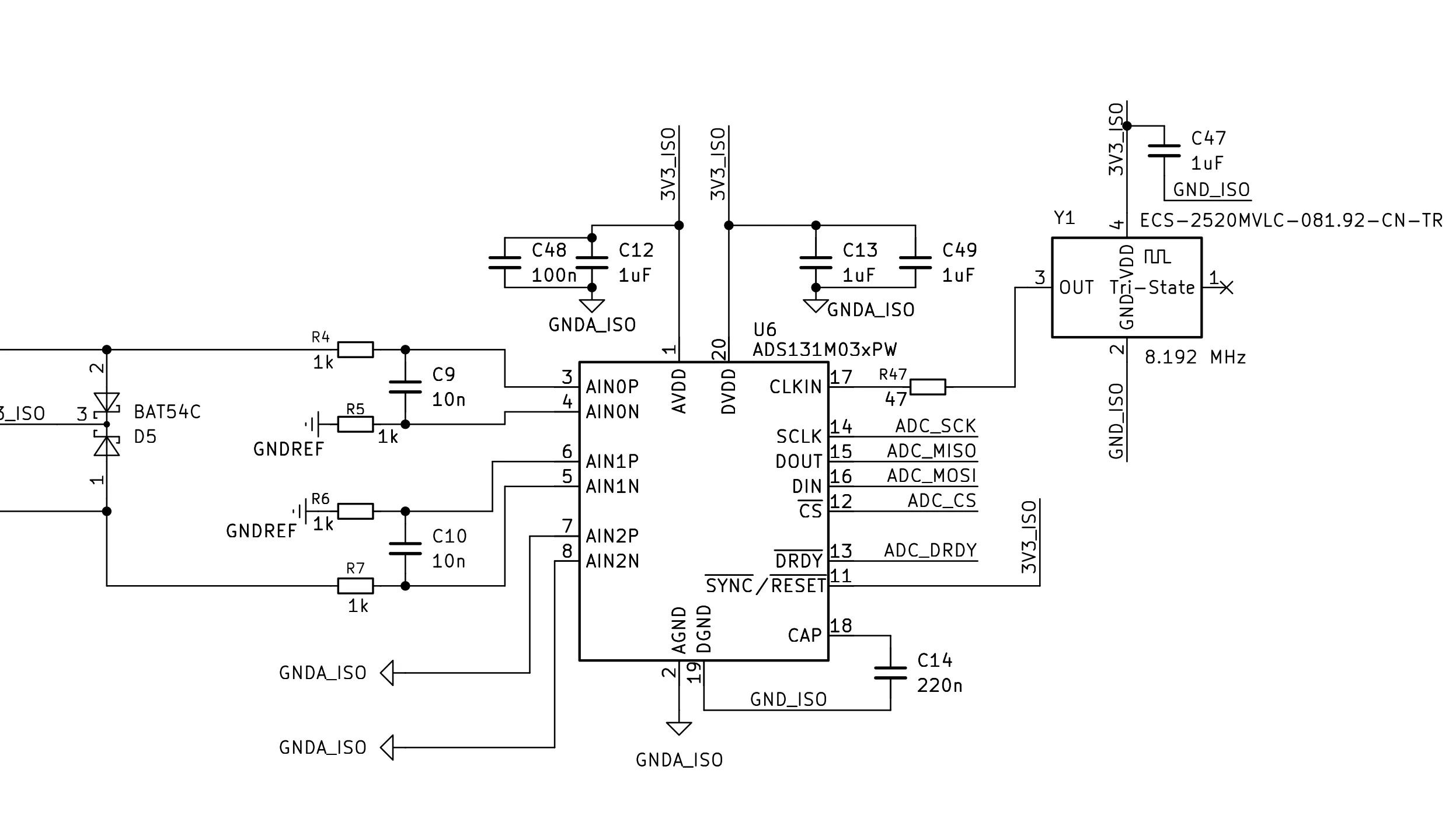
The ADC is a ADS131M02 a delta-sigma 2-channels, 24bits 64kSPS with concurrent sampling. The ADC requires two channels since there are
two amplification branches: one for the nano-amperes and micro-amperes range, and the other one for the milli-ampere range.